UnintegratedCircuit
Part 6 - The Final Schematic & PCB
The Building Blocks
As a quick recap, here are the building blocks that will physically need fitting together for this final circuit diagram:
-
The microcontroller;
-
The high-voltage Nixie PSU module;
-
The Nixie tube;
-
The Nixie tube cathode drivers.
Since the microcontroller is at the centre of the circuit's operation, the schematic was written up so as to reflect this.
The Schematic
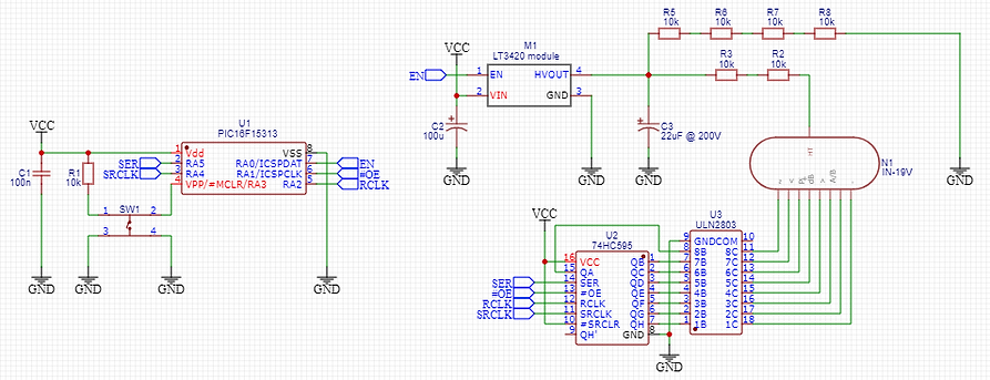
The schematic shown above in Figure 1 is really quite simple and was designed so as to have a minimal Bill of Materials (BoM). This, in turn, helps to minimise costs, as well as the number of components required. In fact, apart from the high-voltage Nixie Power Supply module (and the tube itself, of course), this entire circuit uses low-cost, readily-available components throughout.
The switch SW1 is used as a push-on push-off switch, with the microcontroller toggling the enable signal to the PSU module each time the switch is pressed. The switch's functionality, however, could be altered/extended simply in software (i.e. detecting a press-and-hold situation or a double-press).
The resistors R5 - R8 exist so as to provide a constant load to the high-voltage power supply. This is critical for the stability of the PSU as, under no-load conditions, the voltage comes out of regulation from the nominal 180V up to a peak of over 500V. This could places a lot of stress on the components on the PSU module (the IC, the output capacitor, etc.) and would also massively exceed the voltage rating of the additional electrolytic smoothing capacitor C3. In reality, the Nixie Tube would clamp this voltage to much less; however, the voltage may still increase enough to cause excess current to flow through the tube, shortening its lifespan. The resistance was also chosen (based on trial and error on a breadboard setup) so as to prevent the power supply from switching at an audible frequency, therefore eliminating an annoying high-pitched whine.
Potential Improvements
As this is quite a simple schematic, the scope for improvement is limited; however, one very easy addition would be to add a 6 pin header (male or female) to allow for simple programming/reprogramming of the PIC microcontroller with a PICKIT 3 or PICKIT 4.
Also, one could add some coloured LEDs in series with resistors R5 - R8 if the (somewhat tacky, in my opinion) LED backlighting effect was desired.
The main beauty of this circuit though, is that the effects are all software controlled. This means that changing or adding lighting effects for the Nixie tube can be done almost indefinitely without altering the schematic or PCB at all.
The PCB design
Shown below in Figures 2 & 3 are the top and bottom layers respectively of the final PCB design:


In both figures it is worth noting the extra attention paid to proper separation distances from the high-voltage traces. On this board, high voltages should be confined to the top side of the PSU module (hence no copper cutout underneath the module), the connections to the Nixie tube itself, around the output of the PSU module, and to an extent around the connections to the cathode driver IC (although these are limited to around 50V, so not as bad). Wherever possible, these high-voltage traces have been kept well clear from any low-voltage copper traces/areas since any arcing could not only damage the delicate logic circuitry and potentially any USB power supply, but could also introduce a shock hazard to the user.
Whilst 180V DC (especially at the current capability of the PSU module) is highly unlikely to be lethal to the average person, it is still highly unpleasant, and anyone with a heart condition or similar could face a very real risk of death if exposed to such voltages. As a result, this attention to board layout is paramount.
Another thing of note is the inclusion of two strain relief holes at the top centre of the board. These are not plated thru holes, and are not electrically connected to any part of the board. Their sole purpose is to allow one to thread the positive and negative power wires of a USB cable through them before soldering said wires to the two smaller pads below and to the side. This means that if the USB cable gets pulled for whatever reason, the strain placed on the cable is diverted onto the insulation and against the board rather than directly onto the soldered connection (which could cause the solder joint to break, potentially leading to a short circuit down the line as the loose wire flails around).
Finally, if I was to redesign the PCB, I would ease up on the copper planes, replacing them with a few thick traces instead. Whilst copper planes offer low parasitic resistance and inductance, they are largely unnecessary for low-current, low-speed, non-critical appliations like this. Instead, it just makes it incredibly difficult to solder since, even with a large iron tip and high temperature, the copper draws A LOT of heat out of the iron. This means the probability of a dry joint increases, as well as making adjustments to/removal of components an absolute nightmare.
Conclusion
In conclusion, the schematic is simple to follow and build, and easy to modify; however the PCB design is certainly far from perfect and could definitely benefit from a redesign. The large amount of free space on the top side of the PCB does allow for some PCB artwork in either silkscreen or exposed copper however, which means this could be easily personalised to make a gift for someone (which is precisely the reason I designed this in the first place).
In the next section, I will go over some of the key features of the code for making the 'flicker-flame' effect for the Nixie tube.