UnintegratedCircuit
Part 4 - Testing Efficiency
Efficiency Expectations
In order to get a rough idea of the efficiency that I should be expecting to get, I once again consulted the datasheet and right on the first page under the 'features' overview section it states: "Efficient Flyback Operation (>75% Typical)". There is the benchmark then, 75% efficiency or greater. Additionally, on page 4 of the datasheet, a graph is shown for the example circuit which is identical to my circuit except for component values - this was because of the differing applications. Figure 1 below shows this graph.
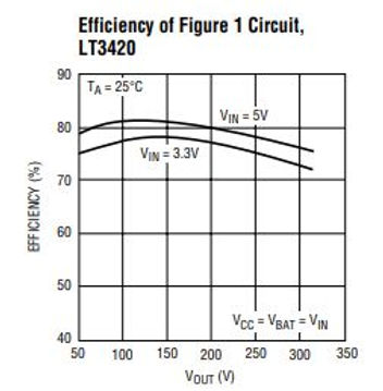
This graph shows approximately 80% efficiency at a VOUT of 180V and a VIN of 5V. It should be noted that this will be the best-case scenario since it will be tested under ideal ambient conditions with a PCB designed by the engineers that developed the IC in the first place and measured with relatively high-profile test equipment.
A final note pertaining to the circuit's efficiency is given on page 15 of the datasheet where it says: "The high voltage operation of the LT3420/LT3420-1 demands careful attention to board layout. You will not get advertised performance with careless layout.".
Setup For Measuring The Efficiency
The setup I used for measuring the efficiency was a bit ugly, to say the least; for starters, I had to design a test load for the circuit, simply changing a resistance didn't work out too well. After a while, attempting to pull more current at the output resulted in dragging the voltage down and, because the load was just a couple of resistors, the resulting current dropped due to Ohm's equation.
This meant that I had to design a high-voltage (180V with headroom) constant current load which would have been fine if any of the transistors immediately available were of a high enough voltage. Sure, there were a couple of IRF730s knocking around but strike one against using them was the fact that they present a highly capacitive load to an op-amp's output which, according to both the datasheets for various op-amps and my own personal experience, does not end well. Strike two is down to the required gate-source voltage. The threshold voltage for the IRF730 could be as high as 4V worst case. Combine that with the USB minimum specification being as low as 4.5V and then factoring in the op-amp voltage swing from the positive rail, this was just not a viable solution.
In the end, I settled on using a TIP41C as the main regulating element; it is a BJT and therefore much more op-amp friendly, requires only about 0.6V to turn on, and, being a BJT, it is almost guaranteed to be more robust to 'mishaps' than a MOSFET equivalent. This transistor only has a collector-emitter voltage of 100V though... My solution... Stick a bunch of TL431s in series with it (I did say this was an ugly setup). Three TL431s were connected in series, each set to have a voltage drop of approximately 30V across them, the end result being that the TIP41C never saw over 100V across its collect and emitter. A schematic of the test load can be found below in figure 2.
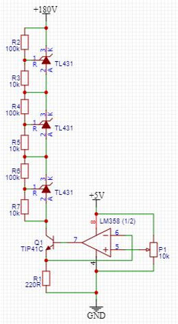
Normally, one could get away with simply using a series resistor or two to reduce the voltage across the transistor; however, this would not work here since the current varies by about an order of magnitude, this would mean having to change the resistance values (and hence the circuit) whilst testing so as to avoid showing more than 100V to the transistor and also to avoid restricting the current through having too high of a resistance (current should be regulated by the transistor only). A test circuit should never be tampered with once tests have begun so as to reduce error introduced by component variation.
The rest of the setup procedure involved using an oscilloscope as a voltmeter to measure the input voltage local to the module PCB (measuring locally is important as explained later on), placing an ammeter in series with the module PCB to measure the input current, and placing an ammeter in series with the test load to measure the output current. The output voltage was of two separate modules was measured prior to any testing and did not deviate from 180V by more than +/- 1V (so about 0.5% error maximum), as a result, the output voltage was assumed to be 180V. With these figures in mind, the input power and the output power can both be calculated for any given measurements.
Procedure For Measuring The Efficiency
The efficiency of the module was measured at different values of refresh capacitance. Before any measurements were taken, the module's upper and lower current limits were tested - a minimum load is required with this module in order to discharge the output capacitor sufficiently so that the refresh period stops charging at the programmed maximum. If no minimum load is provided, the output voltage rises well in excess of the peak reverse voltage on the diode (I have observed about 540V on the output capacitor... I have also touched that 540V through sheer stupidity... Just don't do it).
After having gauged the maximum and minimum currents of the module, a range of test currents common to every refresh capacitance being tested was found, resulting in a 4mA - 12mA output current range. This range was then swept in 2mA increments and, at each step, the input current, local input voltage, and output current were measured and recorded. As already mentioned, the output voltage was assumed to be a fixed 180V.
A series of tables were produced based upon these measurements, as an example, figure 3 shows the table for 100pF of refresh capacitance (as per the original module schematic).
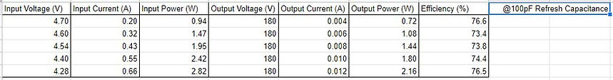
The peak efficiency across all the different output currents and refresh capacitances was measured at 80.5%. These figures would imply an acceptable component selection and PCB layout as the efficiency is approaching the advertised value. a full list of all the tables can be found here. A quick graph summing up the efficiency at the different refresh capacitances is shown below:
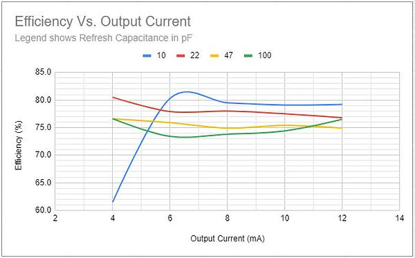
The main issue with this method of measuring efficiency is the lack of regulation of the input voltage local to the module. Because the ammeter uses a shunt resistor, the increasing current flow at higher load currents causes a larger voltage drop across the ammeter meaning a lower input voltage to the module. As can be seen with any common step-up converter, the way to offset a lower input voltage is by drawing more current from the input, hence compounding the problem. As a result, efficiency is probably slightly higher than what is shown in figures 3 & 4.