UnintegratedCircuit
Part 3 - PCB Design
PCB Layout Considerations
When designing power supply circuits, PCB layout is absolutely critical. The consequences of a poor layout are, best case, a notable drop in efficiency (easily 5% or so, could be considerably more) and increased ElectroMagnetic Interference (EMI). Both of these may not be critical for a one-off hobbyist application but if designing for an actual product, these would both be make or break factors. In the worst-case scenario, it could prevent the circuit from working altogether. As frequencies increase, PCB traces stop acting as conductors and start working as inductors & capacitors which in turn form filters which tend to have a rather profound effect on oscillations (namely inhibiting the ones you want and causing ones you do not want).
With all that being said, consulting page 15 of the datasheet yields some information about how to lay the board out; it says: "Keep the area for the high voltage end of the secondary as small as possible.". This was then combined with some other power supply basics:
-
Make high-current traces short and wide. This minimises (I^2)R losses by keeping the trace resistance to an absolute minimum. This also aids in achieving the next point.
-
Keep high-current loops as small as possible. This helps reduce parasitic inductances which will hinder the flow of current at high frequencies, additionally, it also helps reduce EMI.
-
Use a ground plane (a large area of copper entirely dedicated to distributing circuit ground) in order to help reduce the current loop size and reduce electrical noise caused by high switching currents from interfering with the sensitive control and feedback circuitry internal to the IC.
There are a couple of others but these will be omitted since the space constraints of the board did not permit their implementation.

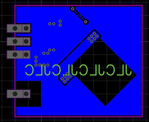
Figures 1 and 2 above show the PCB top layer (left) and bottom layer (right). The resulting PCB is merely 22mm * 25mm (0.85" * 0.97"). Some things to note with the layout include:
-
The bypass capacitor (C1), as well as the other feedback components like the reference resistor (R2) and the refresh timing capacitor (C2), are mounted physically very close to the IC. Ideally, the feedback resistor (R3) would also be located very close to the IC; however, due to using larger 0805 (metric 2012) sized passive components in order to ease the soldering process (by hand with an iron and without magnification in my case) it was impossible to fit them closer - the IC is already surrounded as can be seen.
-
No components could be placed on the rear of the board since this was designed to take male pin headers for breadboard compatibility or to be used as a surface-mountable PCB module.
-
The pads that intersect the edge of the board are doubling up as poor-mans castellations in order to make it easier to solder to when using it as a PCB-mount module. Real castellations would be far better but also add a massive cost to a small, personal use batch like this.
-
The traces leading to and from the transformer are large and short as previously mentioned. The transformer secondary returns to ground via the IC in this case (not a standard affair from what I can tell) hence the trace on the rear of the PCB. This is probably one of the worst things to do but there was honestly very little choice in the matter. The transformer and IC pins for the primary and secondary end up crossing unavoidably. The secondary of the transformer was chosen since the peak current in the secondary is N (the turns ratio) times smaller than the current in the primary.
-
The transformer and diode are mounted at an angle. This is rarely done - but perfectly valid - and was exploited here to minimise the trace length between the transformer and the ic. The diode was then placed at an angle just to help cram it in on the board.
-
The ground plane is removed underneath the transformer to prevent eddy currents being induced in the ground plane which would inject noise into it, cause heating and reduce the efficiency, although these effects would probably be negligible. A large debate between keeping and removing the ground plane underneath an inductor can be found here and effectively sums up the pros and cons of each.
-
Multiple vias are used to 'stitch' ground connections on the top side to the ground plane on the bottom side in order to reduce the impedance, both thermal and electrical, within the circuit.
-
The high-voltage output node is limited to a thick trace as opposed to a copper pour in order to comply with the datasheet that specifies this node should be kept small.
-
There is a large cut in the ground plane surrounding the high-voltage output pad, obviously to improve separation and keep the dangerous high potentials away from the safe USB input (which has a connection to the ground plane).
Even observing all of these layout features, there are bound to be far more qualified people looking at this and cringing at such an awful layout. Regardless, testing shall be conducted... In a future section.