UnintegratedCircuit
Samsung 850 EVO SSD Upgrade
Asus EEE PC 901 Default Storage
From the factory, the EEE PC 901 had some pretty woeful storage options, and the whole system is thoroughly confusing in today's world of SATA simplicity - or even the relatively simple NVME drives, at least from a purchasing perspective. The release of the 901 all but predates the mainstream adoption of SATA, and this is particularly evident from the first time you peruse the relevant section of the device manager.
The 901 has a mind-blowing 12GB of storage... Yup, 12 whole gigabytes. These days, it is difficult to even purchase a USB drive or SD/micro SD card with less than 12GB of storage, let alone an entire machine, although I guess this amount was sufficient in the days of Windows XP. Better is yet to come, however, for it was also split across two physically separate SSDs as shown below in Figure 1, which shows the shorter primary 4GB driver, and longer secondary 8GB drive. According to the 'Specifications' section of the EEE PC Wikipedia page, the Linux versions of the 901 were equipped with 20GB total: a 4GB shorter primary drive, and a 16GB longer secondary drive. These 16GB secondary drives certainly do exist, as there is one currently hiding in my battered 900. The 8GB and 16GB drives are identical save for the number of flash chips populated (all are populated on the 16GB drive, only half on the 8GB drive).

But wait, it gets better yet, these are not SATA SSDs, they actually run through the PATA bus instead, sometimes referred to as the IDE bus, but not here, for reasons which will become apparent later. And just to rub salt in the wounds, these were known as 'PCIE' SSDs back in the day, despite having no relation to the PCIE bus (which does exist in the 901) whatsoever. BUT it still gets worse: despite sharing the physical 52-pin card edge connector with the mPCIE and mSATA cards you may be more familiar with, it actually is not compatible with either. Instead it uses the FLASHCON pinout - essentially a proprietary mass-storage interface developed by ASUS before mSATA became popular and took over. Not only does the pinout not align to anything available today, but neither do the mounting holes (spaced wider apart, and closer to the end than mPCIE/mSATA cards), nor the form factor in the case of the longer secondary drive, at 70mm in length instead of the typical 51mm of the 'standard' cards.
So, hopefully, you now have an appreciation for the absolute mess that is the storage in the EEE PC 901 - not to mention the fact that the two drives operate in a master/slave configuration which means only one drive is ever accessible at any one time. It also makes it annoying to properly install and associate programmes onto the larger secondary drive, although there is a download for a utility by ASUS, still available on their support page under the 'Software and Utility' section, that makes the secondary drive the default install location. I have not yet tested this personally, however.
SSD Upgrade Candidates
Even when the 901s were still in their warranty period, people have wanted to increase their storage - both in terms of size and performance. As per usual, there are many ways to skin a cat. I believe there were some SSDs that served as a drop-in replacement, expanding storage up to 32GB, perhaps even 64GB? These have long since been out of stock, however, and even at the time, I believe they may have been relatively expensive.
People set out attempting to install the deceptively similar mSATA SSDs too. An excellent Russian forum thread has been archived and serves as an excellent resource in a multitude of ways: pinouts, photos of the modification, etc. One of the mSATA modification photos is shown in Figure 2, and although this looks relatively simple, and is (in theory) free, it appears to be plagued by reliability issues, with people reporting their new drive speeds having reduced to 20% seemingly for no reason. Also, for scale, the pads are 0.6mm wide, and the ceramic capacitors are 0402 (imperial) size... Very small stuff which requires very steady hands.

To be fair, if you feel ambitious, this could be a way to go, since modern mSATA SSDs can be had on AliExpress for <£10 at the time of writing (May 2023), so even if it takes a couple of attempts, or fails after a few months, it will not have been a significant financial outlay in the first place.
Additionally, people have been installing Compact Flash (CF) cards for a while now too, since these are also compatible with PATA systems, and the high-end cards can offer ridiculous data transfer rates. There are, again, downsides: they can still be relatively expensive, they have no wear-levelling, they have to be hard-wired in place, and one also has to modify the master/slave selection to set the drive as the new master. Again though, if this floats your boat then go for it, there should be at least a couple of good guides for doing this.
Another way would be to populate the empty footprint for a ZIF-40 socket which would allow one to connect a 1.8" PATA drive - either an HDD, or an SSD. This still requires the soldering of the ZIF socket, however, and the 1.8" HDDs are painfully slow, although do offer decent storage space... But seriously, too slow. The 1.8" SSDs are kind of expensive for what you get, and both are likely either already difficult to source, or soon will be since the 1.8" form factor was never hugely popular. This also requires removing the existing 8GB/16GB secondary SSD to make room for the 1.8" drive, although this likely isn't much of an issue.
And finally, there is the way I will document here: using a Samsung 850 EVO 2.5" SSD... Or rather just the PCB from within. Why? Rationale coming up.
Why the Samsung 850 EVO?
So, why the Samsung 850 EVO in particular? Glad you asked. First and foremost, I discovered from this review by CDRLabs in which they delved inside the 850 EVO case to expose the PCB. It turns out that the 120GB and 250GB versions have a tiny half-slim SATA form-factor PCB inside the much-too-big 2.5" SSD case, as shown in Figure 3 (hope they do not mind I took their photo, full credit to them).

It turns out that this form factor fits almost perfectly on the little plastic shelf (ironically provided to help house a 1.8" drive) with only minimal modification of snipping three of the plastic supports (Figure 5) to allow the protrusion to be recessed through the crossmember. A photo of the test fit is shown in Figure 4.


The second reason was software support - and this is a big one. Windows XP does allow supporting SATA drives in AHCI mode (basically superior to the compatibility/IDE mode); however, it does not support natively sending the TRIM commands to SSDs necessary to keep them in optimal health. I will not divulge too far into the TRIM command, but essentially it allows the SSD's controller to keep track of what blocks of storage are no longer being used (e.g. when a large file has been deleted). Instead of erasing the entire block by writing it with 0s or 1s, and wasting precious write cycles in doing so, it simply overwrites that block next time a new file can make use of it. This essentially prevents the SSD from becoming 'full' and avalanching into poor performance as it runs out of space, desperately trying to shuffle things around behind the scenes, and also, as mentioned, prevents an excessive number of writes to the flash storage, which would wear it out prematurely.
This is where the software support of the 850 EVO comes into play, as an archived version of Samsung's 'Magician' software can be used - the most recent version supported by Windows XP is v4.9.7. This software allows for maual optimisation, as well as being able to detect whether or not the SSD is genuine, and some other useful things, although granted the usefulness appears to be greater in Windows 7 or above where one can enable things like Rapid Mode (or whatever it is called), and 'overprovision' the drive to prevent it from ever becoming bloated and running out of shuffle space. It also contains a simple benchmarking utility to keep track of the drive's speed, and may be a better alternative to CrystaDiskMark (more on that later).
Thirdly, price. I am aware that these are no-longer being produced, but I believe that these SSDs came OEM in many a games console (the XBox primarily, I believe, but citation needed there). As a result, the lower capacity ones, which are the ones with the small PCB which is what is needed here - are still common second-hand for cheap. I got a tested one at >95% health remaining delivered for <£20 (again, May 2023) from eBay, and with the added bonus that all proceeds went to charity. This was for a 250GB unit too. CEX seem to have plenty too, especially in 120GB guise.
Finally, and this was the point of no return for me, ASUS manufactured a handful of modern notebooks which used a 10-pin FPC cable to connect a 2.5" drive to the motherboard in place of whatever was supposed to be there (some M.2 form-factor drive, I believe). This meant that I could actually design my own 'adapter' card PCB to fit into the otherwise useless IDE1 slot (see Nev's blog for more info on this), where the stock primary SSD resides, without the need for a bulky SATA connector and separate hard-wired power. This latter point is a pretty big deal considering that 2.5" SSDs only require a 5V power supply, and the only 5V rail in the 901 is the one that feeds the external USB ports. I even managed to track down a schematic of the relevant motherboard, and some photos too, and derive & cross-reference the pinout of the FPC cable/connector - more info on that soon.
So this is why I chose the Samsung 850 EVO SSD as my weapon of choice for this modification, now onto the implementation...
Designing The Adapter Card PCB
Designing the actual adapter card was not particularly difficult, although it did involve collating and corroborating information from a multitude of sources. My first port of call was to consult the motherboard schematic for the ASUS laptop for which the SATA to FPC cable was intended for. This would give me the pinout of the connector (and thus the necessary signal routing required for the PCB). The pinout is shown below in Figure 6.

As can be seen from the schematic, there is a helpful grouping of three pins (8, 9 & 10), all connected to the +5V supply, this would make life much easier when cross-referencing from the images of the motherboard, as this would allow me to orient the pinout with respect to the connector. Figure 7 shows the relevant part of the 'donor' motherboard.

This gave me all the information required for replicating the pinout. The three commoned pads (+5V) are circled in red, and the series capacitors on the SATA bus differential pairs are circled in cyan. Combining the information in Figures 6 and 7, it transpires that the connector uses the standard 7-pin SATA pinout, with three additional lines for carrying the 5V supply. As a bit of trivia, the three parallel connections are necessary for keeping the maximum current handling through the FPC connector and cable below their rated maximum at 0.5A/line (max current draw of a 2.5" drive is typically 1-1.5A).
The next issue to tackle was the debacle of determining the FLASHCON pinout, since some sources give the SATA RX & TX differential pairs from the host's perspective (i.e. from the SATA control chip's point of view), whereas others give them swapped, thus representing the TX & RX signal from the device's perspective (i.e. from the drive's point of view). This is normally not an issue with SATA connections, since the two differential pairs are abstracted to 'A' and 'B' rather than TX and RX. This was clarified by cross-referencing the mSATA modifications back in Figure 2, with a variety of sources on the mSATA pinout (so as to acquire a majority in agreement). It turns out that the differential traces for the RX pair need to be 'swapped' for the FLASHCON connector to align with the FPC connector, whereas the TX pair can be routed through unchanged.
Next on the agenda was to find an authoritative source for the physical footprint (pad layout) of the 52-pin card edge connector used by FLASHCON, mPCIE, and mSATA. This came courtesy of the 'Mini PCI Express Electromechanical Specification' - I will not link to this PDF, just in case it begins an automatic download - I then copied this layout exactly, and created a custom footprint which should now be published, and therefore available to use, on EasyEDA.
Finally, a simple boost converter was required to step-up the 3.3V rail to a 5V source for the SSD. I opted to use the TPS61023 from Texas Instruments for this purpose since it came in a tiny, highly-integrated package, and could handle the peak current requirement of the SSD. I essentially just followed the typical application circuit in the datasheet, which required only a couple of resistors and ceramic capacitors, plus the inductor. I also opted to follow their recommendation and used a 100µF tantalum capacitor to provide some local bulk capacitance. This is 'required' if there is no existing capacitance in relatively close proximity to the converter's input, since long traces cause high stray inductance which consequently produces a voltage spike if a large inrush current is present. Since I do not know where the closest bulk capacitance is located to the IDE1 socket on the 901's motherboard, and I did not fancy nuking said motherboard, I opted to simply include that extra tantalum. I also added an SMD fuse in series with the input (which is pretty rare for me) to further mitigate sad times.
A few further points of clarification involved the mounting hole positioning, and FPC pin pitch, both of which were measured using a set of digital calipers (my pair resolve down to 0.01mm which is nice).
This culminated in revision 1.0 of my ASUS EEE PC 901 FLASHCON to SATA Adapter Card, as shown in the following section.
Adapter Card PCB - Rev. 1.0
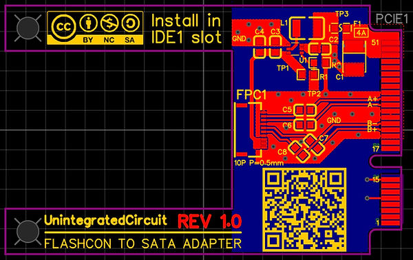

As can be seen from Figures 8 and 9, the final PCB condenses to a neat surface-mount assembly, with a negligible height - important in the confines of the 901's case. The tallest component is actually the tantalum capacitor. One concept, inspired by Figure 2 was to use the series capacitors in the SATA lines to enable the 'B' lines to be crossed without having to jump between the copper layers - something which ruins things like impedance and trace matching.
In the end I neglected to worry about trace width and spacing for differential impedance matching to the SATA specifications since the traces are relatively short and direct. One thing I did prioritise was the trace length matching between the '+' and '-' signals within each differential pair. The total trace length difference in each pair was kept well below 1mm. Trace length matching between pairs is not so important - especially given the maximum capability of SATA-1 speeds, which the ICH7-M (specifically the 'M' for 'Mobile' version) operates at.
The silkscreen gives clear indications of what is what, with the exception of the 'B+' and 'B-' markings by the card-edge connector which have been put on the wrong way around. Just to clarify the traces are connected correctly, only the silkscreen is incorrect. This has been corrected for revision 1.1.
The next section is a 'user guide' for the PCB, including where to install it, and what values to measure on the test point pads. A complete bill of materials is included in Table 1 below as well - all components used were available from LCSC at the time of writing meaning one might even be able to exploit JLCPCB's assembly service too, especially considering this only requires assembly on one side of the board.
PCB Assembly & Usage Guide
First off, when it comes to assembling SMD PCBs, I prefer to get the complicated bits over with early. This often means mounting the fine-pitch components first - in this case, that's the FPC connector and the boost converter IC. The FPC connector can likely be done by drag soldering the 10 fine pins on the 'back' with a regular soldering iron after soldering the two 'anchor' pads on either side. If assembling in this manner, I would recommend traditional lead-based solder for its lower melting point since it is all too easy to melt the plastic body of the FPC connector. Alternatively, solder paste and a hot air gun can be used (which is the approach I took). It is imperative that the maximum temperature of the plastic body is not exceeded though - the datasheet soldering profile recommends an absolute maximum of 250°C for 3 seconds, and at least 230°C for up to 40 seconds. Following this logic, if you can obtain a solder paste that melts below 230°C, then simply set the hot air gun at 230°C and just wait for the paste to melt. Keep the airflow relatively low so that the connector does not get blown away and start a small way away from the board to preheat it before moving closer to melt the solder in a timely manner.
The rest of the assembly is relatively straightforward and can be completed with a soldering iron and some patience.
In terms of testing after assembly, the following should be observed:
-
DMM set to continuity - approximately 0Ω between pin 51 of the mPCIE card edge connector and TP3. This ensures the SMD fuse has not failed open circuit.
-
DMM set to continuity - high resistance/over-range TP3 and GND. This ensures that there are no short circuits on the input side of the boost converter.
-
DMM set to continuity - high resistance/over-range TP1 and GND. This ensures that there are no short circuits on the output side of the boost converter.
-
DMM set to voltage - approximately 3.3V should be measured betwen TP3 and GND. This verifies that power is reaching the card and the boost converter, as well as verifying that the SMD fuse has not failed open circuit.
-
DMM set to voltage - approximately 5V should be measured betwen TP1 and GND. This verifies that the boost converter is operating as intended.
-
DMM set to voltage - approximately 0.6V should be measured betwen TP2 and GND. This can be used to help diagnose issues (i.e. if the load is removed and the output voltage is still not reaching 5V, a faulty IC could be the cause).
Obviously, it should go without saying that voltage measurements must be done with the card installed, and the motherboard powered. This can be done completely outside of the laptop with relative ease, just make sure to place a clean sheet of paper on your working area to prevent stray balls of solder or snippets of wire from causing a short circuit on the motherboard. This is not a great deal of additional effort, especially as the tactile switch under the power button is already on the motherboard.
The next section shows where to install the adapter card, as well as what it looks like fully assembled and installed. For tutorials on how to remove the motherboard, I recommend reading through parts 1 and 2 of Bit-Tech's tutorial.
Installation
To install the adapter card in the intended IDE1 slot, a fair level of disassembly is required as the motherboard needs to be removed to gain access to the IDE1 slot.
To remove the motherboard, and install the adapter card the following will need to be done:
-
Main battery needs to be slid out
-
Bottom maintenance hatch/RAM cover needs to be unscrewed and popped off
-
WiFi antennas need to be popped off of the WLAN card
-
The keyboard needs to be popped out, and have the flex connector disconnected
-
The various plugs and flex connectors under the keyboard must be removed (i.e. speakers, fan, touchpad, etc.)
-
The screws from under the keyboard must be removed, and the palmrest/top half of the chassis prised up and popped off
-
The LCD cable connector should be popped off
-
The two screws (one located by the outer edge of either screen hinge) should be removed
-
The motherboard will need to be removed, pull up the side with the 3.5mm aux jacks and single USB first, and then slide the VGA port side out from its recess.
-
Flip over the motherboard and unscrew the two screws holding in the primary SSD in the IDE1 slot.
-
Install the flex cable from the ASUS SSD kit into the FPC connector on the adapter card.
-
Install the Adapter card into the IDE1 slot, feeding the flex cable underneath one of the 'arms'
Reinstall the motherboard, including its screws, making sure that the SATA SSD connector does not get 'lost' in the process. Once the motherboard is reinstalled, the Samsung 850 EVO SSD can be plugged into the SATA SSD connector, and taped into place. I used Kapton tape (the transparent yellow stuff, also heat-resistant), so that it is easy to see if the Samsung 850 EVO is still in place and properly secured. Functionally, standard electrical insulation tape will also work just fine, but obviously without the quality-of-life feature of being able to still see the SSD. Some form of insulation must be provided though, and it must cover the entire top of the Samsung 850 EVO PCB, since the RAM hatch features a metalised film (for EMI suppression) on its inside surface - you do not want to short circuit anything here. Given that the Samsung 850 EVO PCB must also be secured, it seems logical to kill two birds with one stone, and use a suitable insulating tape.
If I find the time, memory, and willpower, I might add photos or a YouTube video, detailing the installation procedure.
Conclusion
Wrapping up this section then, I can tell you from experience that this is a very worthwhile modification, and was also a very successful one. Somehow, my adapter PCB was able to successfully carry full SATA 1 speeds, and it was actually this which bottlenecked the Samsungs 850 EVO SSD to a speed of approximately 130MBps read/write. This is 4-5 times faster than the stock FLASHCON SSDs. One extra interesting finding when running CrystalDiskMark was that, when the CPU was underclocked (i.e. when using the power saving profile of the Asus Super Hybrid Engine), the reported disk speed actually increased. My assumption is that CrystalDiskMark might be using a clock source which is altered when underclocking, thus causing it to record more read/write transactions per 'tick' of this clock source.
Finally, if sufficient demand is there, I may consider making and selling small batches of these adapter cards over on eBay or Etsy. Otherwise, I may consider uploading the design files here such that folks can make their own.